The KRI KDC75 ion source is equipped with defocused molybdenum grids and an automatic controller. The source is installed into a custom built vacuum system for ion beam milling. After installation, a set of experiment was performed to assess the uniformity of the milling system.
The process parameters for the mill is listed in the table below. After the system has reached base pressure, the process gas if turned on and the source discharge was enabled and is allowed 5 minutes to warm up. After milling the source is turned off and the process gas remains on for another 15 minutes to cool the source before venting.
Base Pressure [Torr]
5x10⁻⁶
Ar [sccm]
7
Discharge Voltage [V]
40
Discharge Current [A]
1.1
Beam Voltage [V]
600
Beam Current [mA]
120
Accelerator Voltage [V]
120
Accelerator Current [mA]
6.6
Neutralizer Voltage [V]
9.9
Neutralizer Emission [mA]
133
Sample Distance [cm]
15
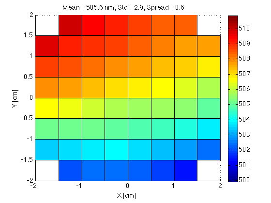
The experiments are performed using a silicon wafer with approximately 500 nm of thermal oxide. Shown in Figure 1 is a map of oxide thickness across a wafer. The thickness of the oxide is measured using a J.A. Woolam M-2000 spectroscopic ellipsometer. The average thickness of the oxide is approximately 505.6 nm with a spread of 0.6%. Interestingly, the oxide thickness appears to increase monotonically along an axis. When the wafer is rotated 180°; and measured again, the results are consistent.
Figure 1: Map of oxide thickness across a 3" wafer.
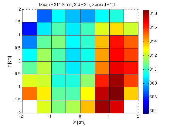
Figure 2 is a map of oxide remaining after 300 seconds of milling. The remaining oxide is approximately 311.8 nm thick with a spread of 1.1%. Although the spread increased slightly, the thickness variation across the map is different.
Figure 2: Map of oxide remaining after 300 seconds of milling.
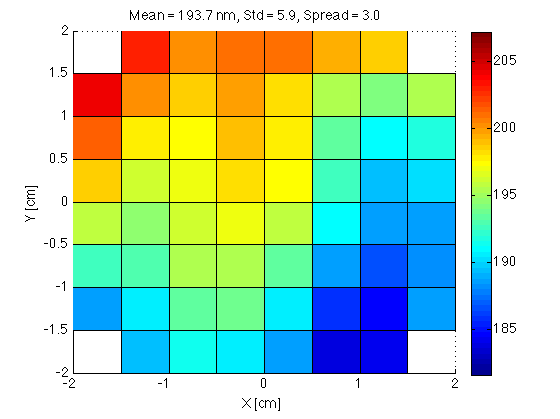
Figure 3 is a map of the amount of oxide removed after 300 seconds of milling. Figure 3 is essentially a difference of Figure 2 and Figure 1. The milling rate is not uniform and it appears to be slightly tilted. After milling approximately 193.7 nm of oxide, the removed film thickness varies by 3%. Interestingly, we thought that non-uniform heating of the sample during milling would have some effect on the milling uniformity. The sample is mounted on the holder such that the left half is in contact with the holder while the right half is suspended. Perhaps mounting the sample in this fashion does not have a significantly influence mill uniformity.
Figure 3: Map of removed oxide after 300 seconds of milling.
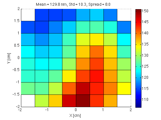
Figure 4 is a map of oxide remaining after 600 seconds of milling. The remaining oxide is approximately 129.8 nm thick with a spread of 8%. Since the milling uniformity is slightly tilted, it is reasonable that the oxide thickness uniformity degrades with increased mill time. In fact, the standard deviation for a 600 second mill is nearly double of the standard deviation for a 300 second mill. Also, the remaining oxide map pattern in Figure 4 and Figure 2 is consistent with the milling pattern from Figure 3.
Figure 4: Map of oxide remaining after 600 seconds of milling.
From the two milling experiments, we are able to calculate an etch rate for thermal oxide of 0.65 and 0.63 nm/s for milling times of 300 seconds and 600 seconds respectively. Since the milling rates are effectively the same, the process of warming up the source for 300 seconds does not seem to mill the wafer.