Core Technology
Core technology is developed to continuously improve the capabilities of the lab so that researchers can hit the ground running with their projects. A core technology can take an experienced professional weeks, months or years and significant resources to develop. Core technology development must be properly documented to teach valuable research and development skills, share practical mistakes and observations, and generate more return on investment. UHNF core technology is shared openly to promote our capabilities and support our community.
Core Technology Development
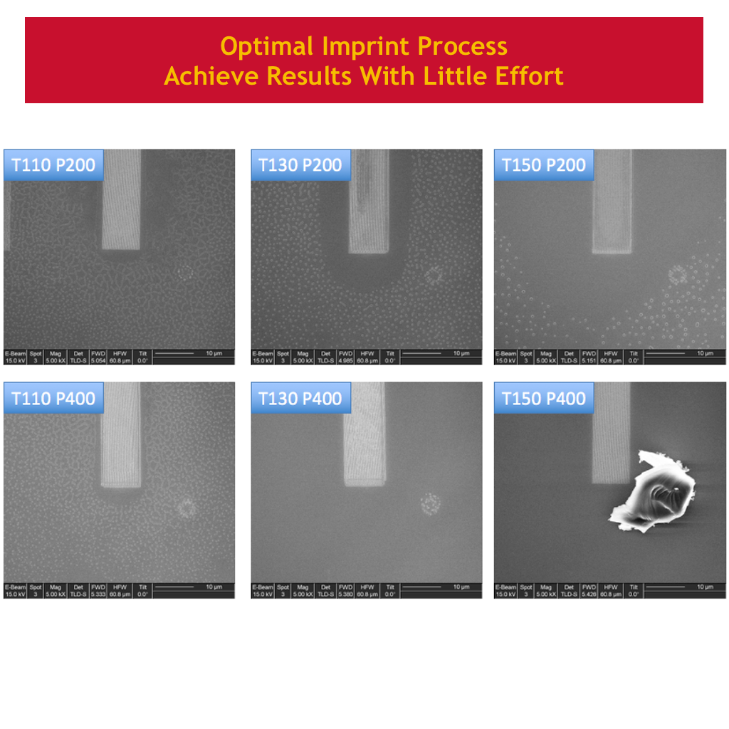
The cost of core technology development depends on experience, skill, knowledge and core technologies. For example, after the installation of the nanoimprint tool, some basic training from the manufacturer, a few independent experiments and some discussion with experienced researchers, it was evident that the practice of nanoimprinting is far more difficult than advertised. As it turns out, it took approximately 1 year to develop the supporting core technologies needed to develop a procedure to reliably perform nanoimprinting that can be taught to new researchers in 30 minutes.
The development of this technology has lead to the following new capabilities:
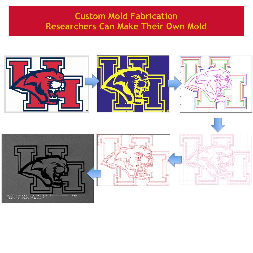
- Custom Mold Fabrication
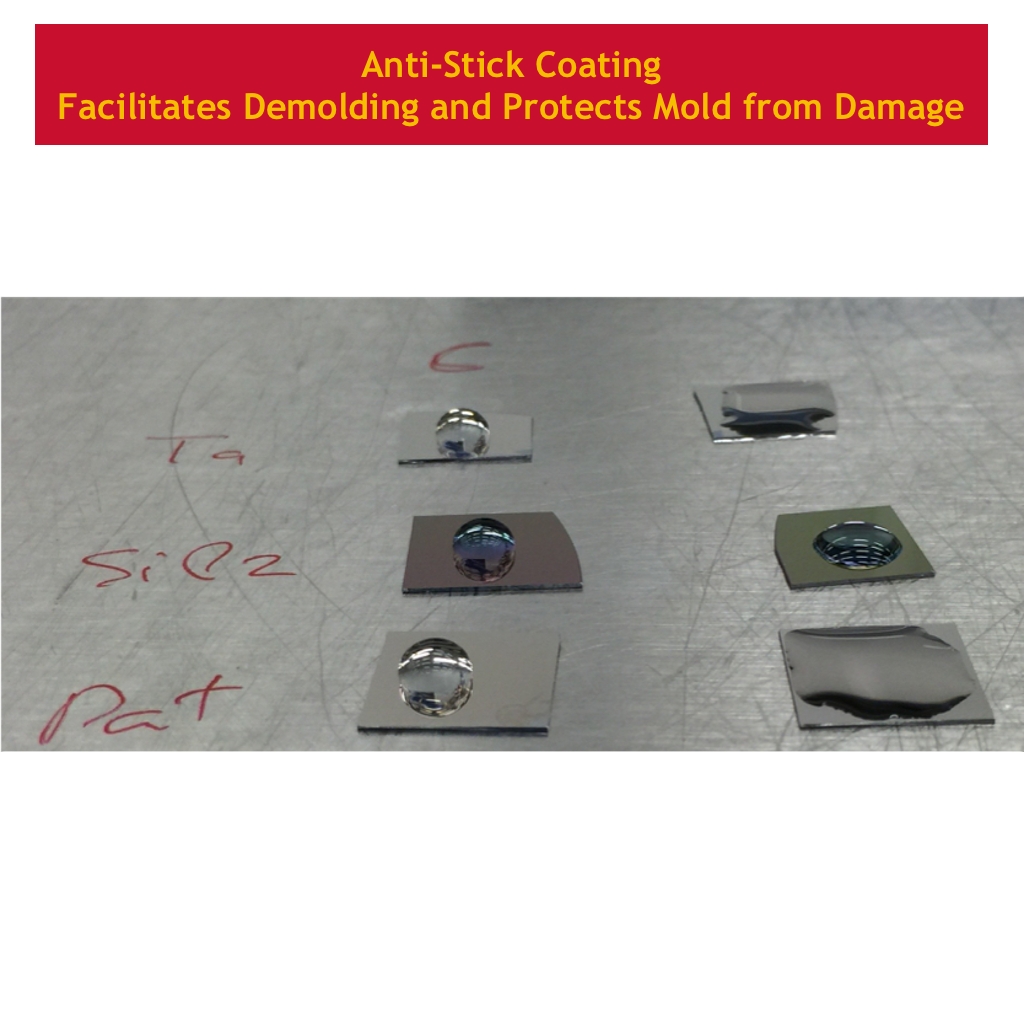
- Anti-stick Coating
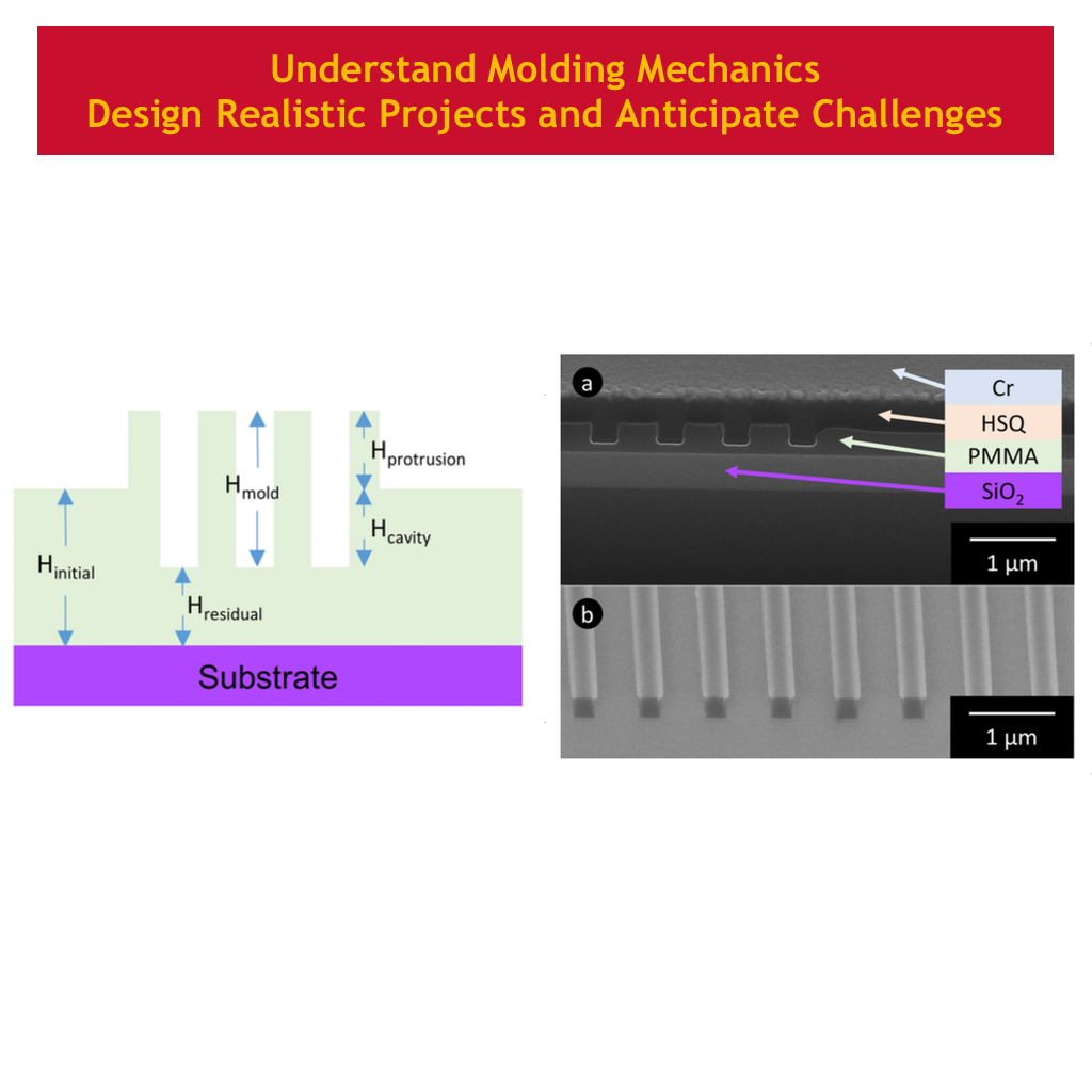
- Thermal Nanoimprinting with PMMA
- Mold and Sample Cleaning
In addition, UHNF staff has acquired expertise in thermal nanoimprinting technology. This allow us to provide more accurate research advice and more easily troubleshoot user problems.


Core Technology
Name | Description | Technology |
---|---|---|
PMMA | PMMA is a positive tone electron beam media with below 30 [nm] resolution and a sensitivity of 400 [uC/cm2]. PMMA costs $1/mL and has an infinite shelf-life. | Electron Beam Lithography |
MMA/PMMA | MMA/PMMA comprise of a layer of MMA beneath PMMA. MMA/PMMA is a positive tone electron beam media with below 60 [nm] resolution and a sensitivity of 400 [uC/cm2]. MMA/PMMA costs $2/mL and has an infinite shelf-life. The pattern produced in the MMA layer is always wider than the PMMA layer by at least 60 [nm]. This undercut greatly improves the lift-off process. | Electron Beam Lithography |
HSQ | HSQ is a negative tone electron beam media with below 30 [nm] resolution and a sensitivity of 700 [uC/cm2]. This resist costs $25/mL and has a 6 month shelf life. | Electron Beam Lithography |
PHOST | PHOST is a negative tone electron beam media with below 200 [nm] resolution and a sensitivity of 15,000 [uC/cm2]. This is a cheaper and more stable alternative to HSQ. | Electron Beam Lithography |
AZ1512 | AZ1512 is a positive tone UV media with below 2 [um] resolution and a sensitivity of 50 [mJ]. AZ1512 costs <$1/mL and has an infinite shelf life. | Photolithography |
Adhesion on Silicon | Photoresist does not adhere to hydrated silicon surface. Here we explore various approaches to improve photoresist adhesion. | Photolithography |
Glass Mask | A plastic mask cost up to 10 times less than a glass mask. Here is a low cost process to transfer a flexible mask pattern onto a glass mask. | Photolithography |
Lor5A/AZ1512 | LOR5A/AZ1512 comprise of a layer of AZ1512 above a layer of LOR5A. After patterning, the LOR5A pattern will always be wider than the AZ1512 pattern. This undercut greatly facilitates the lift-off process. | Photolithography |
SiO2 Mold | Standard nanoimprint molds are expensive and there are currently no companies offering molds with custom patterns. Here we describe the procedure to fabricate nanoimprint molds in SiO2. This process works with all forms of SiO2 such as thermal oxide or fused silica wafer. | Nanoimprint Lithography |
Tone Reversal | In thermal nanoimprint, a rigid mold pattern is imprinted into a thermoplastic polymer such as PMMA by pressing the mold into the polymer while applying heat. The heat softens the thermoplastic, allowing it to be displaced from the protruding areas in the mold. Nanoimprinting requires higher pressures and temperatures as the ratio of protrusions to cavities increases. This problem can be avoided by using this tone reversal process to transform cavities in the thermoplastic to protrusions. | Nanoimprint Lithography |
Anti-Stick Coating | A nanoimprint mold must be protected with an anti-stick coating to prevent contamination by the imprint media. This process produces a teflon-like coating that is effective for molds with 100 [nm] minimum features. | Nanoimprint Lithography |
Mold Replication | Nanoimprint molds are very expensive and are subject to extreme abuse during the imprint process. The master mold can be replicated to form many identical sub-master molds. | Nanoimprint Lithography |
PMMA | PMMA is a thermoplastic that is imprinted at 500 [psi] and 150 [°C] | Nanoimprint Lithography |
HSQ | HSQ is imprinted at 500 [psi] and room temperature | Nanoimprint Lithography |
mr-I | mr-I is a thermoplastic that is imprinted at 500 [psi] and 90 [°C] | Nanoimprint Lithography |
XY Drift | The XY stage drift is characterized for the Asylum Research MFP-3D Origin+ atomic force microscope. | Atomic Force Microscopy |
Z Drift | The Z actuator drift is characterized for the Asylum Research MFP-3D Origin+ atomic force microscope. | Atomic Force Microscopy |
Variable Field Module | The variable field module is characterized for the Asylum Research MFP-3D Origin+ atomic force microscope. | Atomic Force Microscopy |
Source Meter Integration | A Keithley 2400 source meter was integrated into the Asylum Research MFP-3D Origin+ atomic force microscope to provide resistance measurements. | Atomic Force Microscopy |
TEM Sample Preparation | Learn the procedure to prepare a sample for TEM | Focused Ion Beam |
Particle Manipulation | Learn the procedure to pick up a 500 nm particle and place it anywhere you want | Focused Ion Beam |
SiO2:HSQ | This process etches SiO2 and HSQ at approximately the same rate. | Reactive Ion Etching |
PMMA:HSQ | This process etches PMMA, but does not appear to etch HSQ. The lateral etch of PMMA is also characterize to control the undercut depth. | Reactive Ion Etching |
Si:AZ1512 | This Bosch process etches Si 30 times faster than AZ1512. | Reactive Ion Etching |
Si:AZ1512 Post | Silicon (Si) and AZ1512 have very different chemical composition. This document the process development steps taken to produce 7 [µm] diameter and 50 [µm] tall silicon posts. | Reactive Ion Etching |
SiO2:Cr | This process etches SiO2 and Cr at a rate of 377 and 6.9 [nm/min] respectively. | Reactive Ion Etching |
SiO2:HSQ | This process etches SiO2 and HSQ at a rate of 126 and 204 [nm/min] respectively. | Reactive Ion Etching |
SiO2:PMMA | This process etches SiO2 and PMMA at a rate of 29 and 29 [nm/min] respectively. | Reactive Ion Etching |
SiO2:mrI7000R | This process etches SiO2 and mrI7000R at a rate of 25 and 12 [nm/min] respectively. | Reactive Ion Etching |
SiO2:AZ1512 | This process etches SiO2 and AZ1512 at a rate of 45 and 13 [nm/min] respectively. | Reactive Ion Etching |
Si:AZ1512 | This process etches Si and AZ1512 at a rate of 2858 and 325 [nm/min] respectively. | Reactive Ion Etching |
Si:PMMA | This process etches Si and PMMA at a rate of 330 and 156 [nm/min] respectively. | Reactive Ion Etching |
PMMA | This process etches PMMA at a rate of 70 [nm/min] | Reactive Ion Etching |
mrI7000R | This process etches mrI7000R at a rate of 64 [nm/min] | Reactive Ion Etching |
NXR1025 | This process etches NXR1025 at a rate of 55 [nm/min] | Reactive Ion Etching |
Anti-Stick Coating | This process deposits an anti-stick coating | Reactive Ion Etching |
Photoresist Adhesion Promotion | This process dehydrates the surface of a silicon wafer to improve photoresist adhesion | Reactive Ion Etching |
Base Pressure | The base pressure is an important process parameter. The trace gases are characterized for the AJA ATC-2200. | Sputtering |
Uniformity | The deposition uniformity is an important process parameter to control to ensure homogenous material properties across an entire wafer. The uniformity depends on the gun angle, gun position and throw distance. The uniformity is characterized for the AJA ATC-2200. | Sputtering |
System Geometry | The system geometry provides a path towards modeling the deposition uniformity and rates. | Sputtering |
Thickness Data | The spin coating thickness can vary depending on the environment and sample size. Our experiences show that the film thickness is approximate half of what is shown in the manufacturer datasheet. This document contains the spin speed vs film thickness data for PMMA, HSQ and AZ1512. | Spin Coating |
Adhesion Promoter | Adhesion promoters are applied to improve the adhesion of a spin coated film to a material. In this report, we explore various products to improve the adhesion of AZ1512. | Spin Coating |
Maximum Process Time | The maximum process time for the Allwin21 Accuthermo AW410 varies with temperature. The process time is not limited for temperatures up to 650 [°C]. At higher temperatures, the process time decreases rapidly to 80 [s] at 1050 [°C]. | Rapid Thermal Processing |
Uniformity | The ion milling uniformity is an important process parameter to characterize to ensure an entire wafer is milled at the same rate. | Ion Milling |
Rate Calculator | Use this rate calculator to estimate the ion milling rate for your material. | Ion Milling |