When an electron beam writing system is calibrated, the beam will be in focused on the sample surface. When the sample surface is above or below the focal point of the beam, the writing accuracy and precision degrades. Variability in the sample surface position will result in variability in the size and position of the written pattern.
An electron beam writer should be equipped with an automatic height compensation system. This system uses an infrared laser and detectors to maintain a fixed sample height by raising or lowering the stage. Unfortunately, not all electron beam writers are equipped with a height compensation system. These instruments are much more reliant on precision engineering, frequent calibration and years of characterization in order to achieve a comfortable level of confidence. The fees for using an electron beam writer ranges from the low hundred to many thousands of dollars. Without a height compensation system, the equipment is prone to a number of problems that cannot be reliably solved with significant skill and research and development.
Surface Flatness
For the 3 inch prime wafer, the SEMI specification for total thickness variation is 25 [μm]. The total thickness variation is a measure of the difference between the maximum and minimum thickness values across a wafer. A 3 inch prime wafer also has other specifications for flatness such as bow (40 [μm]) and warp (40 [μm]).
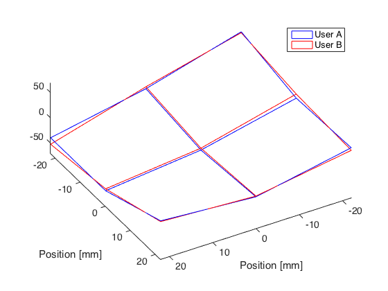
The actual surface flatness needs to be measured after the sample has been loaded into a cassette to acquire a height map. Figure 1 is the average height map for a 3″ Silicon wafer loaded using the 3″ wafer cassette. For the JBX5500FS electron beam writer, the height map for each sample size and cassette is different, but it is repeatable. Once the height map is measured, it can be used to instruct the electron beam writer to compensate for focus errors on the sample. This approach for height compensation does not provide the comfort of an automatic height compensation system. Also, is it safe to assume that a predefined height map for a bare Silicon wafer will be the same as a processed wafer? Will a third or fourth user produce the same height map? What if something changed with the cassette? Considering the cost of using the equipment, the uncertain performance is unnerving.
Pattern Size Variability
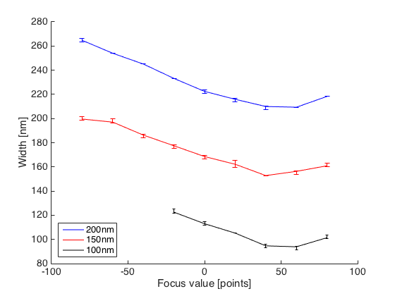
The beam size varies when the sample surface is above or below the focal point. The same effect is achieved by keeping the sample surface at a fixed position and changing the focus value. The size of the beam effects the resolution of the print. For example, we have printed 400 [nm], 200 [nm], 150 [nm] and 100 [nm] periodicity line gratings with 50% duty cycle. The patterns are printed on a sample consisting of Si/SiO2(500nm)/PMMA(115nm). The patterns are exposed at 400 [uC/cm2] using M4_A2_1nA (Mode 4, Aperture 2, 1 nA). The focus value is varied from -80 [points] to 80 [points]. The grating patterns are printed within 100 [μm] of each other to ensure negligible difference sample height.
Figure 2 is a plot showing the width of the exposed line patterns as a function of focus value. The minimum width for the line patterns are found at a focus value of 40 and 60. Below 40 points and above 60 points, the width of the line patterns increases. This trend is observed for all three sizes of gratings. It is also important to realize that the best focal value is approximately 50 [points] above the calibrated focus value. When performing calibration, the electron beam writer will focus on the focus mark which apparently is not at the same height as the sample. Focusing on the sample is better than focusing on the focus mark, but keep in mind that the sample is not flat.
Positioning Variability
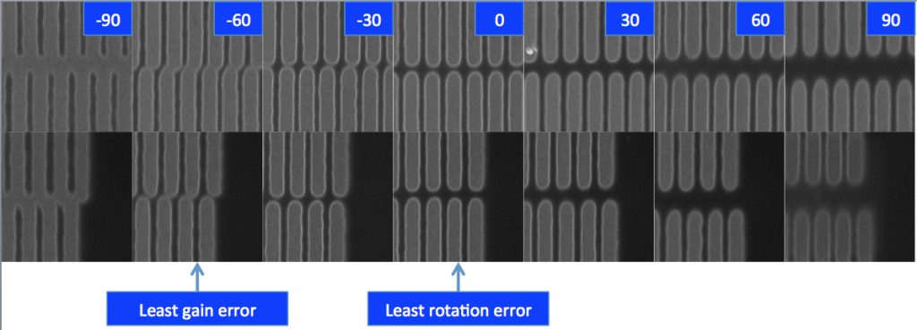
The electron beam writer draws patterns on a 2D plan by deflecting the beam at an angle. The deflection calibration is performed on the BE mark, so if the sample is further away than the BE mark, then the same deflection will result in a wider scan. In addition, the scan field will also be rotated. The influence of focus on deflection errors can be investigated by printing the pattern shown in Figure 3.
Figure 3 shows 12 grating patterns (200 nm pitch with 50% duty cycle) printed using M2_A2_1nA (Mode 2, Aperture 2, 1nA) at a dose of 350 μC/cm2. The patterns are designed such that half of each grating belongs in one field and the other half belongs in a different field. In addition, the gratings that crosses a vertical field boundary are horizontal lines and the gratings that crosses a horizontal field boundary are vertical lines. If there are any imperfections in stitching the fields, it will be revealed at the field boundaries where the patterns are expected to match.

Figure 4 shows the seams for vertical grating patterns at different focus points. As the focus point increases from -90 to +90, the patterns are initially overlapped and gradually moves apart. This is indicative of the field size shrinking as the focus value increases and, on the contrary, the field size increases as the focus value decreases. The focus value also affects the rotation of the field, which is revealed by the misalignment of the gratings. The rotation error is easily observed when looking at the edge of the gratings. In this experiment, the rotation error is approximately 0 at a focus value offset of 0. At positive focus value offsets, the rotation is counterclockwise; and at negative focus value offsets, the rotation is clockwise.
After carefully analyzing the image and assuming a linear relationship between focus vs gain and rotation, we determined that:
- Field rotates by 0.0027 degrees counterclockwise per +30 focus points.
- Field shrinks by 135 nm per +30 focus points.