Processes
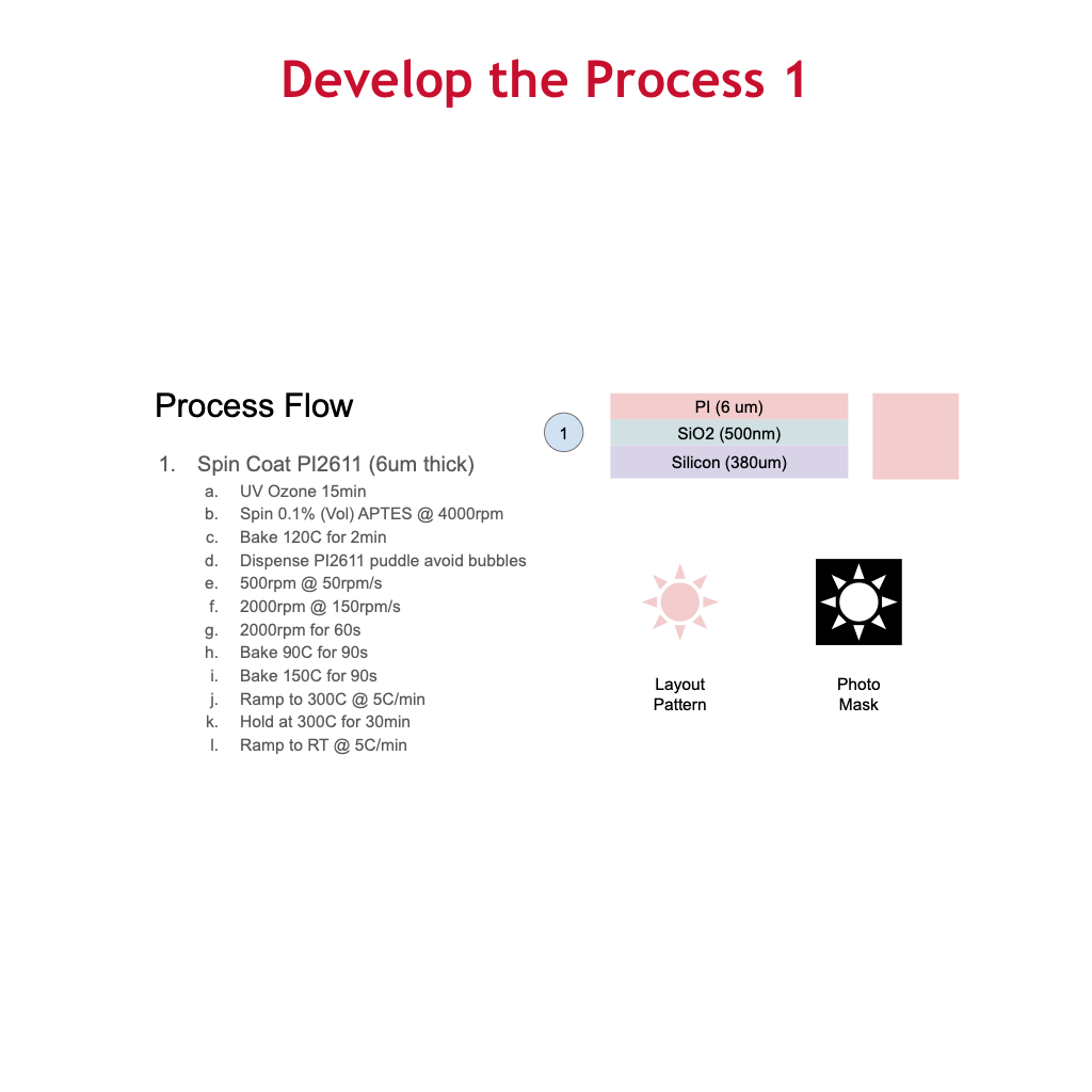
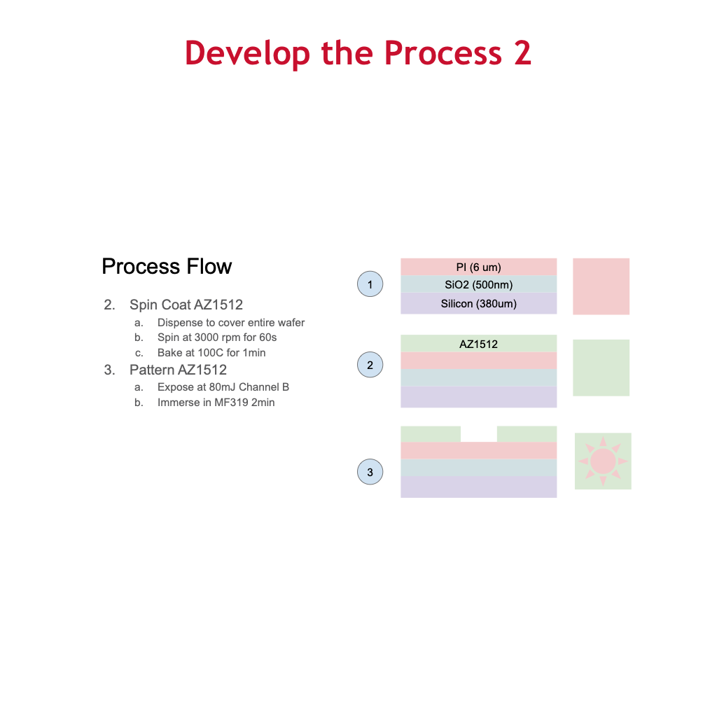
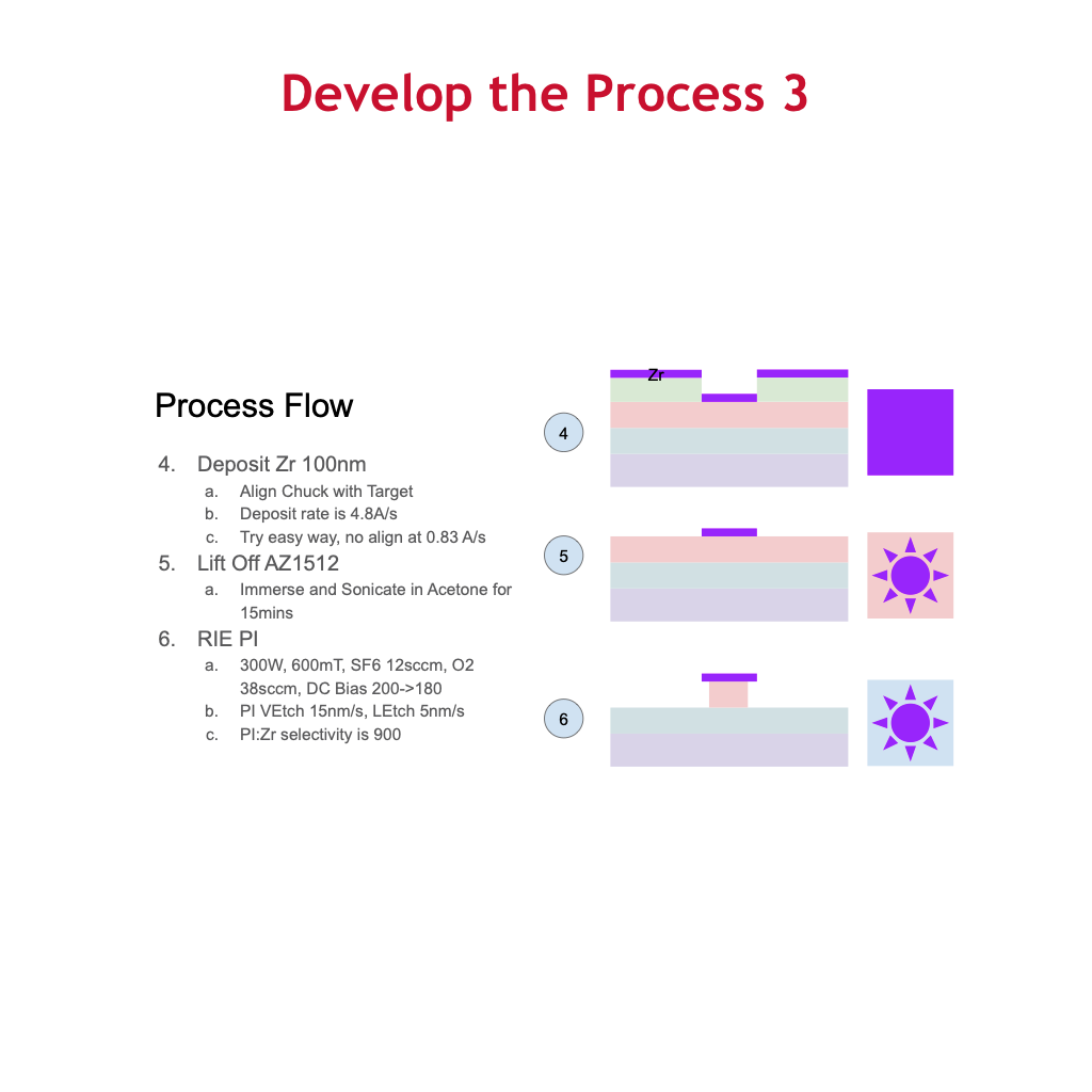
Processes are the building blocks for microfabrication. The fabrication of a device involves performing a number of processes in a particular order. Device fabrication becomes challenging when new processes are needed. Developing a single new process may take weeks, months or years depending factors such as knowledge, skill, resources, and specification. However, once a process is expertly developed and well documented, it can produce the specified results by any operator. As a microfabrication facility matures, the capabilities and level of productivity of its members are associated with the quality of its process database.
The first ascent of El Capitan took 47 days. Modern climbers can do it in 4-6 days using a variety of known paths, while the most elite climbers did it in just under 2 hours! Similarly, the UHNF process database enables many devices/projects to be completed much more quickly.
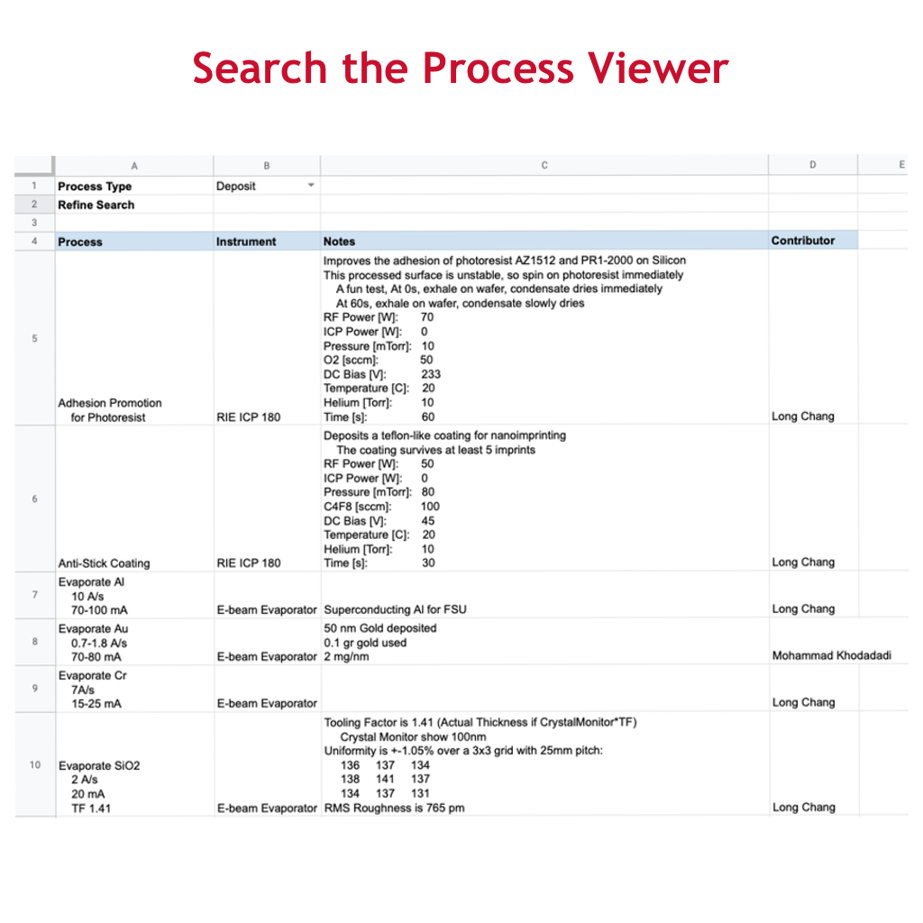
The Process Viewer is a searchable database maintained by UHNF. Use this to develop the procedures to fabricate your device.
1. Select a Process Category
Selecting the process category (deposit, etch, pattern, etc) will show all processes in that category. New users should browse through the results to learn how processes are named and described in the process field.
2. Refine the Search
Enter keywords such as material names to refine the search. This searches through the process field of the results.

Video Introduction
Core Technology
| Name | Description | Technology |
|---|---|---|
| MMA/PMMA Bilayer Resist | MMA/PMMA is a bilayer electron beam resist where the MMA layer is beneath the PMMA layer. After exposure and development, MMA patterns are approximately 120 [nm] wider than PMMA patterns. This feature is great for producing clean structures via lift-off. | Electron Beam Lithography |
| PMMA/HSQ Bilayer Resist | PMMA/HSQ is a bilayer electron beam resist where the PMMA layer is beneath the HSQ layer. Electron beam lithography is used to pattern the HSQ layer. Then a reactive ion etcher is used to etch through the PMMA layer while the HSQ layer is unaffected. This process provides excellent control over the amount of undercut in PMMA. | Reactive Ion Etching |
| SiO2/HSQ Etch | HSQ is a material that can easily be patterned that shares similar qualities to SiO2. From this experiment, we discover that the ICP Power can be selected to achieve an etch selectivity between SiO2 and HSQ of 1 to 1 or 0.6 to 1. | Reactive Ion Etching |