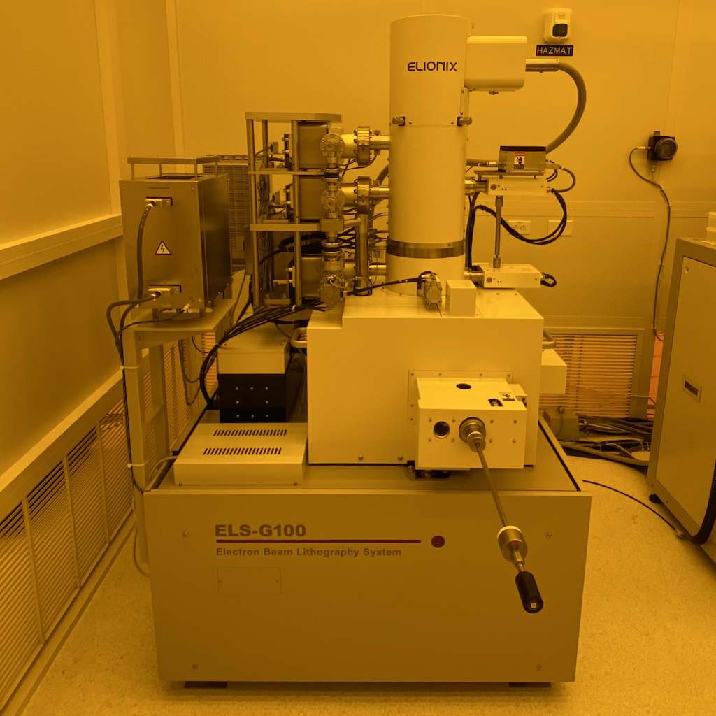
| Beam Positioning | An electron beam lithography system uses a series of lenses to force a beam of electrons to land accurately and precisely on the sample. Accuracy refers to the likelihood an electron lands at the target and is defined by the terms beam drift, deflection error and field distortion. Higher accuracy is achieved by providing a stable operating environment and more frequent calibration. |
| Beam Shaping | An electron beam lithography system uses a series of lenses to force a beam of electrons to land accurately and precisely on the sample. Precision refers to how tightly each electron clusters at the target and is defined by the terms beam size and beam shape. Conventionally, the beam is considered to have a Gaussian shape and the beam size is specified as the full-width half maximum (FWHM) of the Gaussian distribution. The beam shape is actually elliptical instead of circular, so it is defined more completely as the FWHM of a Gaussian distribution along the X and Y axis. In general practice, the beam size and beam shape is optimized either by focusing to produce a sharp image of a resolution target or executing a focusing routine. |
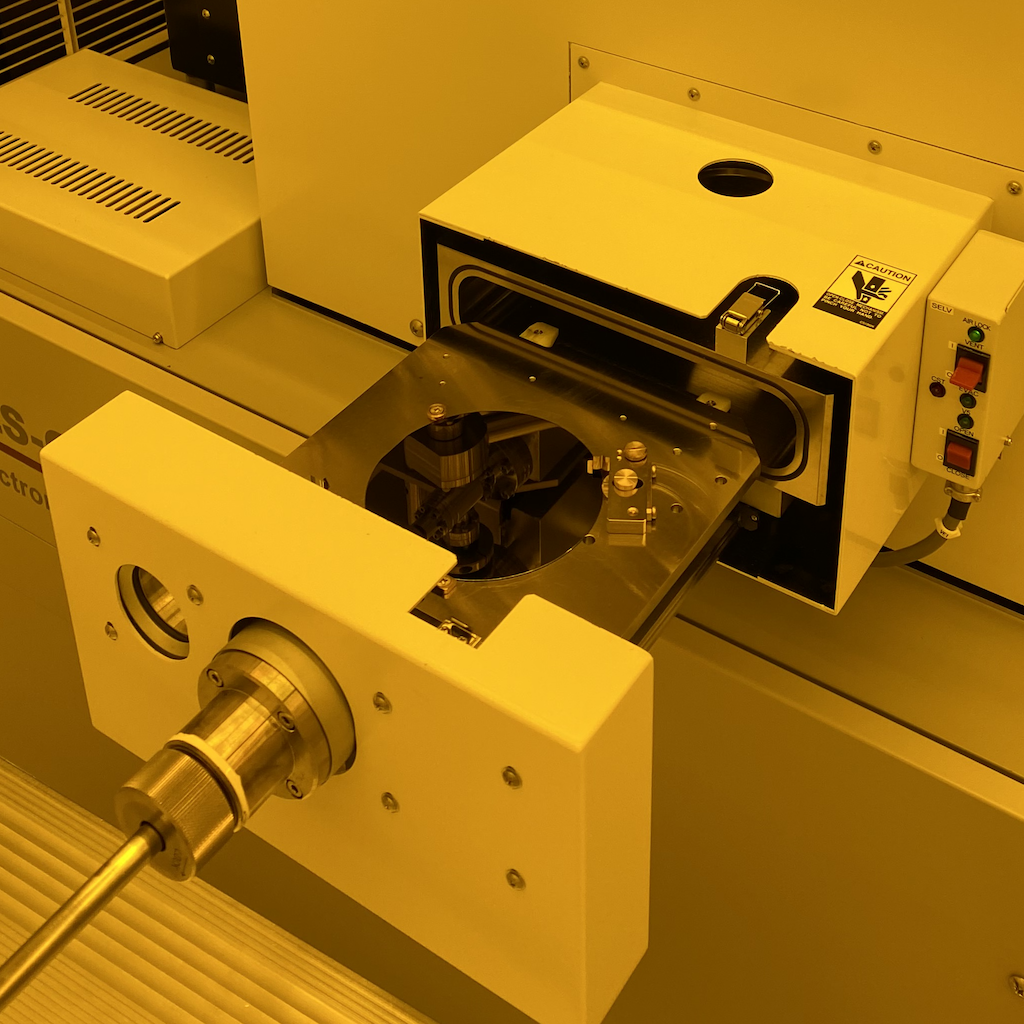
| Height Compensation | When an electron beam writing system is calibrated, the beam will be in focused on the sample surface. When the sample surface is above or below the focal point of the beam, the writing accuracy and precision degrades. Variability in the sample surface position will result in variability in the size and position of the written pattern. |
| Pattern Fracturing | An Electron beam writer exposes a shape by discretely scanning a focused electron beam across a primitive shape (primitives). Designers produce CAD patterns that resemble their device. These CAD patterns must be fractured or decomposed into primitives before it can be handled by an electron beam writer. Understanding the process that converts a CAD pattern into primitives provides some control over how the pattern is written. |
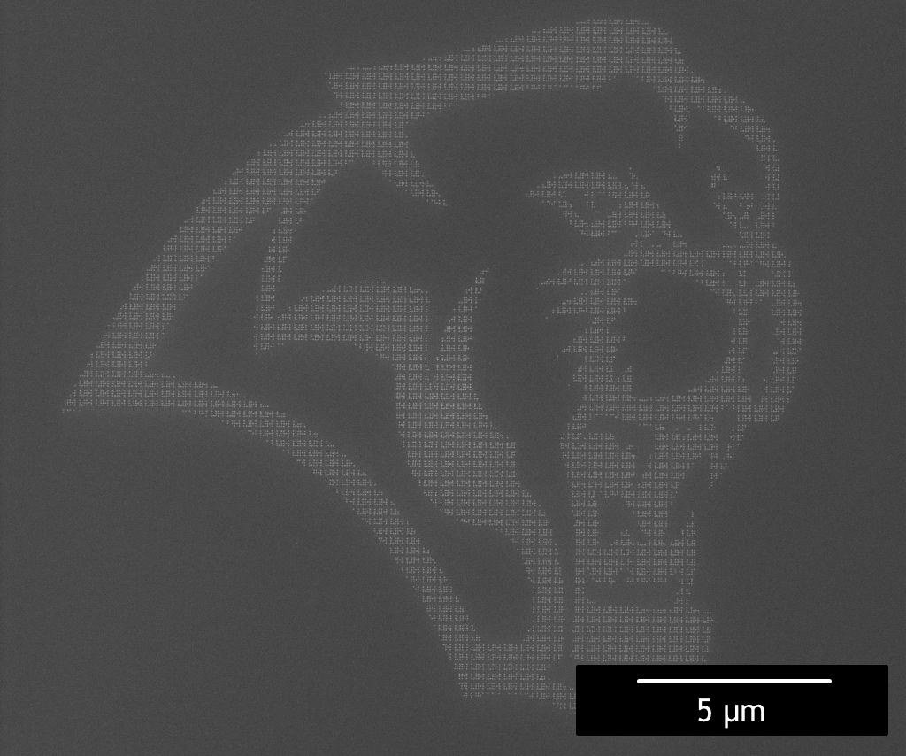
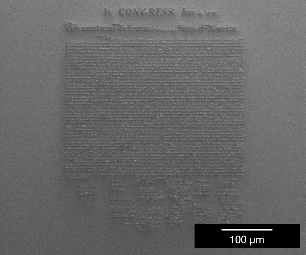
| Proximity Effect | The proximity effect is a major challenge for electron beam lithography. Patterns in electron sensitive resists (eFilm) are created by exposing the eFilm to a beam of energetic electrons. Like how a projectile may ricochet and hit the same target multiple times, an electron can expose the eFilm multiple times. The additional exposures after the first one arise from uncontrollable mechanisms and are collectively called the background exposure. Severe background exposures cause prints that differ from the layout. |
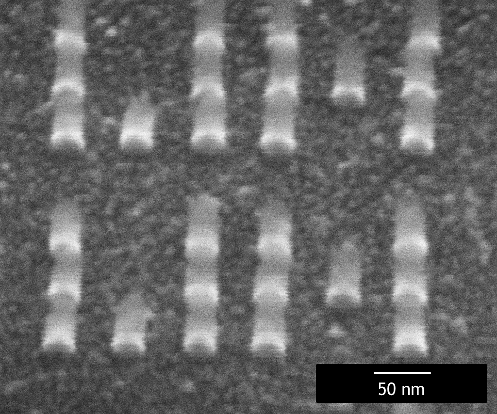
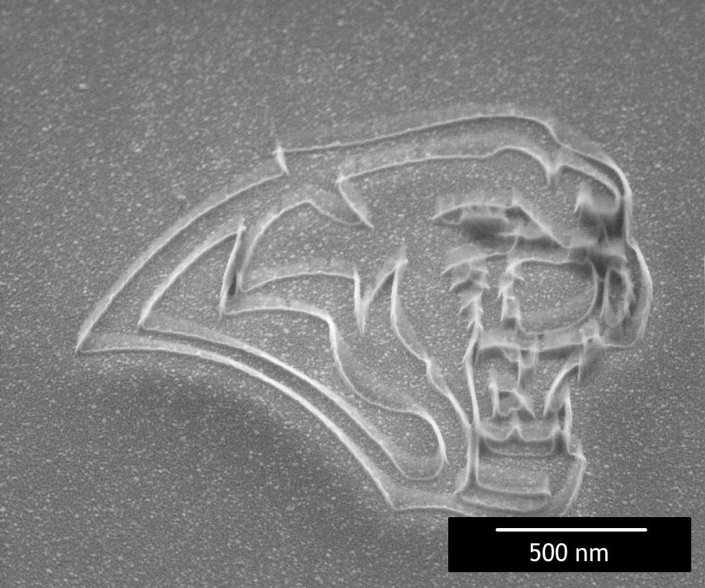
| Writing | An electron beam writer exposes a shape by discretely scanning a focused electron beam across the pattern. This produces a shot pattern that fills the shape. Typically the spacing between each shot is smaller than the beam size resulting in a solid exposure of the shape. Shapes are exposed one by one until the entire pattern is complete. |