MMA:PMMA Bilayer
The MMA:PMMA bilayer electron beam resist system can be useful for processes that require lift-off. MMA and PMMA develops in the same solvent, 2:1 IPA:water. However, the critical dose for MMA and PMMA is approximately 100 [uC/cm2] and 400 [uC/cm2] respectively. This property can be exploited to achieve some control over the amount of undercut, but the proximity effect limits the kinds of patterns that can be fabricated.
Objective
Determine the limitations of the MMA:PMMA bilayer system. What mechanisms limit the resolution and density?
Design of Experiment
- Use a Silicon substrate
- Spin on 100 nm of MMA(8.5)MMA Copolymer
- Spin on 100 nm of PMMA
- Expose grating patterns using electron beam lithography
- Grating patterns are 100, 200, 400, 1000 nm wide with 25% and 50% duty cycle
- Dose is 450 μC/cm2
- Develop by immersing in IPA:Water (2:1) for 1 minute
- Ebeam evaporate 80 nm of Cr
- Use a focused ion beam to inspect a cross-section of the pattern
- Measure pattern width
- Measure undercut width
- Lift-off by immersing in acetone for 5 minutes
- Use FIB to inspect the chrome pattern
Results
25% Density Grating Patterns
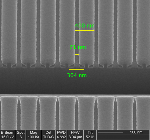
Figure 1 shows a scanning electron image of a cross-section of a 100 nm wide grating with a pitch of 400 nm. The annotations reveal that the grating width is 71 nm, the pitch is 400 nm and the undercut width is 115 nm. The grating width may actually be larger than what is measured because there is 80 nm of Cr evaporated on the sample. Nonetheless, it is evident that the MMA layer dissolves more than the PMMA, resulting in an undercut that is 200 nm wider than the exposed pattern.

Similar results were observed for 200 nm wide gratings with a pitch of 800 nm and 400 nm wide gratings with a pitch of 1600 nm. The table below summarizes the results. From this experiment, the least amount of undercut observed is 65 nm.
| Design Width [nm] | Dose [uC/cm2] | Measured Line Width [nm] | Measured Undercut Width [nm] |
| 100 | 300 | 40 | 65 |
| 200 | 300 | 142 | 65 |
| 400 | 300 | 369 | 90 |
| 100 | 450 | 70 | 115 |
| 200 | 450 | 180 | 106 |
| 400 | 450 | 398 | 122 |
50% Density Grating Patterns
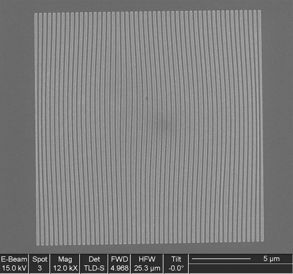
At higher density, the proximity effect becomes more dominant making it more difficult to expose the PMMA layer without over exposing the MMA underlayer. Figure 2 shows a 200 nm grating pattern with a 400 nm pitch. In other words, we have 200 nm of exposed PMMA separated by only 200 nm of unexposed PMMA. This pattern was exposed at 450 [uC/cm2] so assuming an undercut of 106 nm, the MMA layer beneath the unexposed PMMA should be complete gone. Without the MMA fixing the pattern to the substrate, the unexposed PMMA is free to move resulting in a grating pattern that looks distorted. At a dose of 300 [uC/cm2] the 200 nm grating pattern looks better, but there are still some minor defects resulting from the delamination of the unexposed pattern.

It is clear that the proximity effect is a huge challenge for this process, limiting its use to low density patterns. There are certainly many options in an electron beam lithographer’s toolkit that can be used to push the limits of the MMA:PMMA bilayer system such as proximity effect correction, critical point drying, and process optimization. If undercut with a positive tone electron beam resist is a necessary process, then another option may be the PMGI:PMMA bilayer process. However, each process has its caveat and we have not discovered any easy bilayer undercut process for a positive tone resist. For a negative tone resist, the PMMA:HSQ bilayer process works perfectly.
Lift-Off
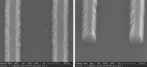
Figure 3 shows the chromium pattern after lift-off. The chromium pattern looks clean with no tearing defects along the edges. The pattern has a taper that is caused by the electron beam evaporation process. The width of the tapered edge measures approximately 32 nm for the three different grating size (100, 200 and 400 nm).
