The MMA:PMMA bilayer electron beam resist system can produce nanoscale structures with clean edges via lift-off. This happens because the same process that produces patterns in PMMA will produce slightly oversized patterns in the MMA layer underneath. This undercutting of the MMA layer allow materials to be deposited into the patterned area without touching the sides of MMA and facilitates the dissolution of the MMA and PMMA during lift-off.
Objective
Determine the limitations of the MMA:PMMA bilayer system.
Design of Experiment
- Begin with a 3″ Silicon substrate
- Spin on 100 [nm] of MMA(8.5)MMA Copolymer
- Dispense MMA(8.5)MMA EL3.6 across entire wafer
- Spin at 3000 [rpm] for 60 [s]
- Bake on a hotplate at 180 [ºC] for 120 [s]
- Spin on 100 [nm] of PMMA 950K
- Dispense PMMA950 A4.5 across the entire wafer
- Spin at 3000 [rpm] for 60 [s]
- Bake on a hotplate at 180 [ºC] for 120 [s]
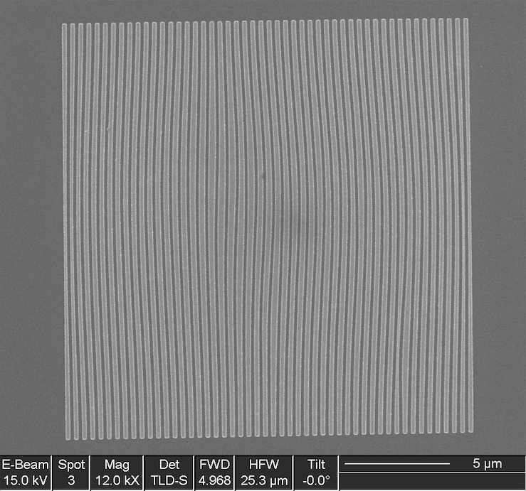
- Expose grating patterns using electron beam lithography
- Grating patterns are 100, 200, 400, and 1000 [nm] wide lines with 25% and 50% duty cycle
- Dose is 300 and 450 [μC/cm2]
- Develop by immersing in IPA:DI Water (2:1) for 1 minute
- E-beam evaporate 80 [nm] of Cr
- Use a focused ion beam to inspect a cross-section of the pattern
- Measure pattern width
- Measure undercut width
- Lift-off by immersing in acetone for 5 minutes
- Use a focused ion beam to inspect the chrome pattern
Results and Discussion
25% Density Grating Patterns
Figure 1 shows a scanning electron image of a cross-section of a 100 [nm] wide grating with a pitch of 400 [nm]. The annotations reveal that the actual grating width is 71 [nm], the pitch is 400 [nm] and the undercut width is 115 [nm]. The grating width may actually be larger than what is measured because there is 80 nm of Cr evaporated on the sample. Nonetheless, it is evident that the MMA layer dissolves more than the PMMA during development, resulting in an undercut that is 200 nm wider than the exposed pattern.
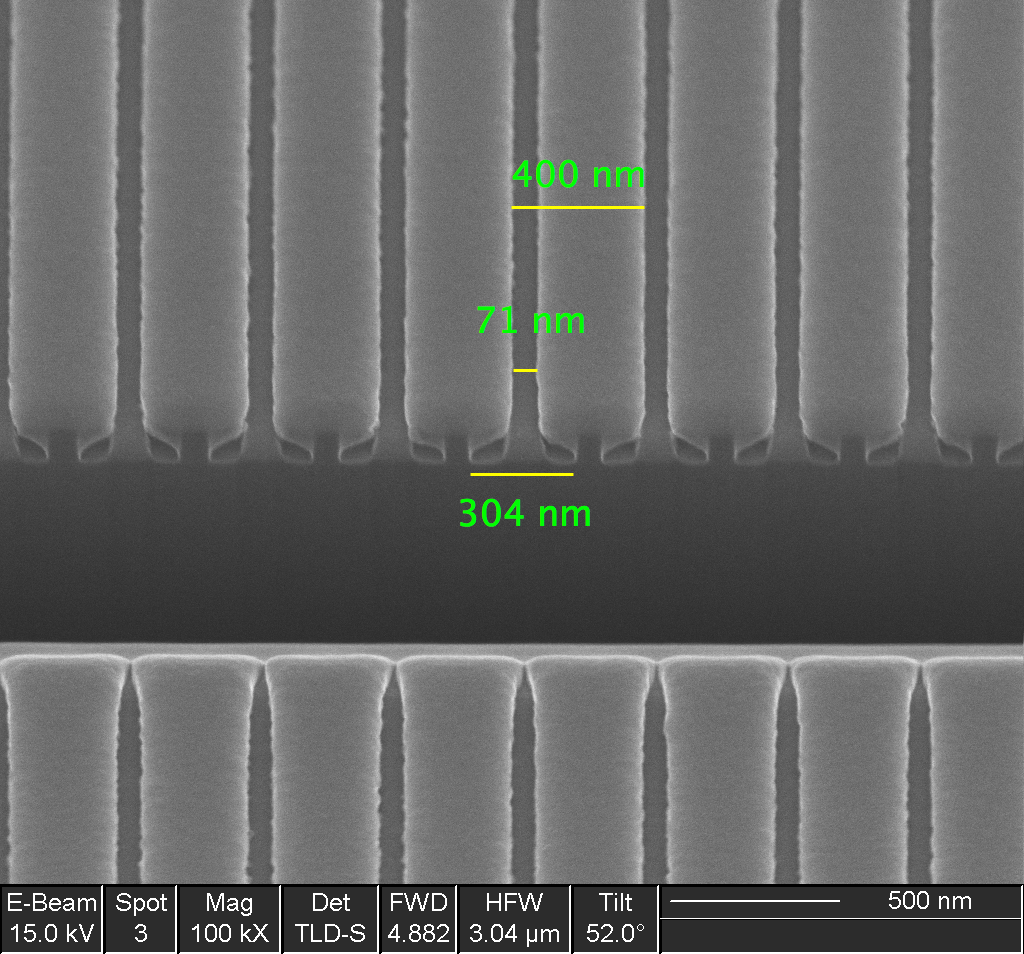
Similar results were observed for 200 nm wide gratings with a pitch of 800 nm and 400 nm wide gratings with a pitch of 1600 nm. The table below summarizes the results. From this experiment, the least amount of undercut observed is 65 nm.
| Design Width [nm] | Dose [uC/cm2] | Measured Line Width [nm] | Measured Undercut Width [nm] |
|---|---|---|---|
| 100 | 300 | 40 | 65 |
| 200 | 300 | 142 | 65 |
| 400 | 300 | 369 | 90 |
| 100 | 450 | 70 | 115 |
| 200 | 450 | 180 | 106 |
| 400 | 450 | 398 | 122 |
50% Density Grating Patterns
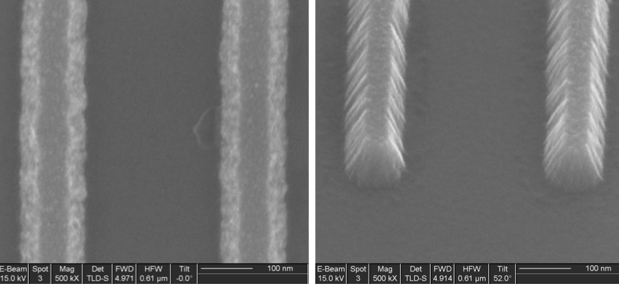
Lift-off
The chromium pattern looks clean with no tearing defects along the edges. The pattern has a taper that is caused by the electron beam evaporation process. The width of the tapered edge measures approximately 32 nm for all three different grating size (100, 200 and 400 nm).