Microfabrication deposition technology provide engineers and scientists access to every known material and also enable the development of new materials. High purity material are often deposited in a controlled environment with atomic precision. Multiple materials can be combined through mixing, layering, or other means to tune the behavior of the material.
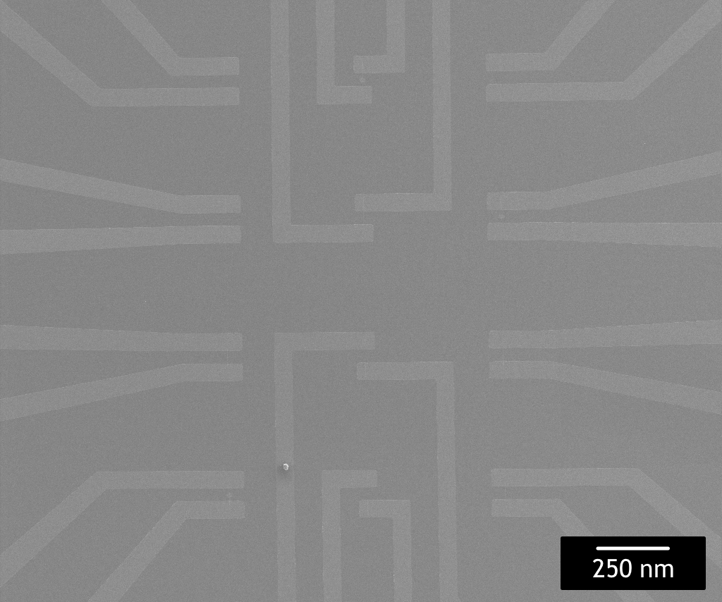
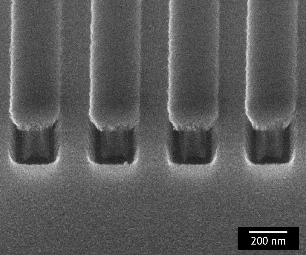
Deposition is often combined with lithography and etching to provide material contrast. For example, a gold film can be deposited and then patterned into channels to direct the flow of electrons through a defined path. This process allow nanoscale structures to be produced using a variety of materials depending on the desired function.
Sputtering
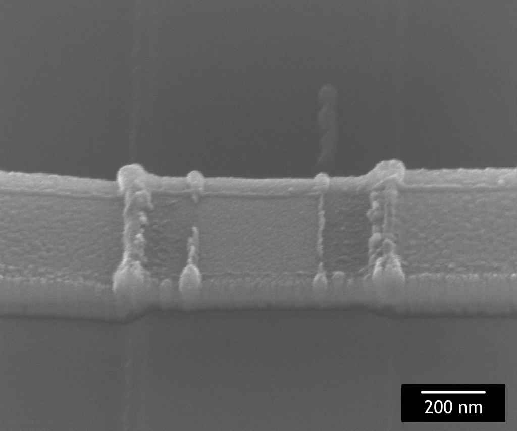
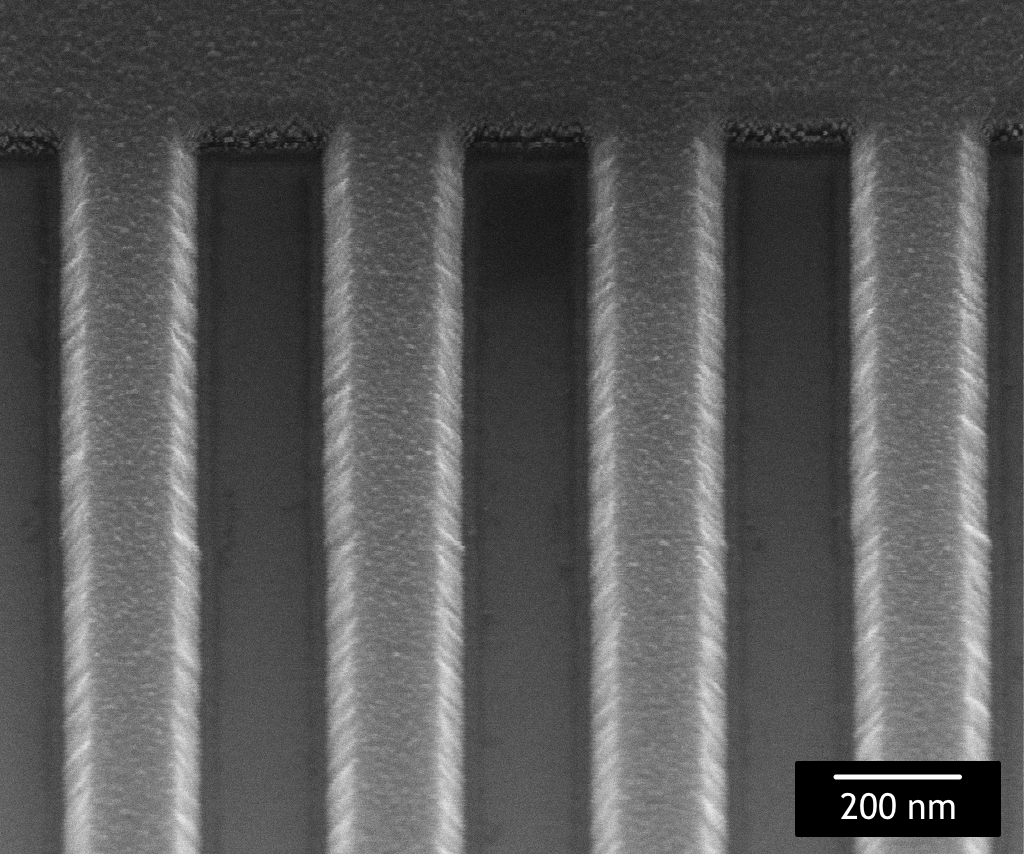
Sputtering bombards a pure target material using a heavy and noble element such as Argon. This process ejects atoms from the surface of the target material towards a substrate in a controlled environment. As the atoms land on the substrate, it can move around until it runs out of energy and sticks to the surface. The target atoms tend to pile up on the substrate surface to form atomically smooth films.
Sputtering can produce extremely pure films of single elements, layers of different elements, and/or composites of specifiable stoichiometry. The material properties can be additionally controlled by varying the environment during deposition or through post processing. Sputtering equipment tend to produce conformal coatings which conforms to the contours of the substrate surface.
Electron beam evaporation melts a pure target material using a beam of high energy electrons focused into a point. This process raises the temperature of the target material in a vacuum environment until the target atoms can escape the surface through evaporation or sublimation. Some of the escaped atoms will fly directly towards a substrate and stick almost immediately. The target atoms tend to pile up on the substrate surface to form atomically smooth films.
Electron beam evaporation can produce extremely pure films of single elements, layers of different elements, and/or composites of fixed stoichiometry. The material properties can be additionally controlled by varying the environment during deposition or through post processing. Electron beam evaporation equipment tend to produce directional coatings that only deposit on substrate surfaces that has direct line of sight of the evaporation source.
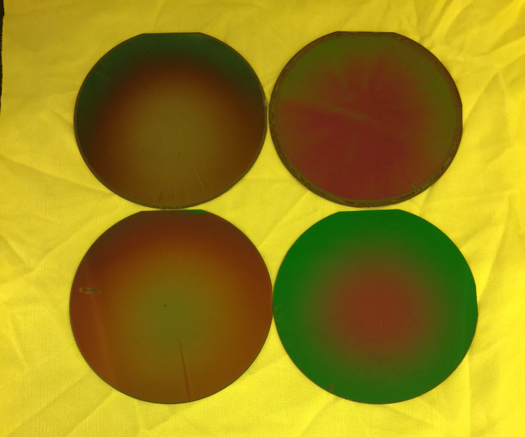
Spin coating spins a substrate to spread a puddle of solution. The solution comprise of a solid material such as a polymer dissolved in a solvent. During spin coating the puddle of solution spreads across the substrate surface and forms a thin coating. Following a baking step on a hot plate, the solvent completely evaporates from the coating leaving behind a thin film of material.
Spin coating can produce extremely uniform films with homogenous properties from a liquid source. Spin coating is typically used to coat a substrate surface with a thin film of polymers. Layers of different polymers can be coated in sequence if the correct solvents are used.
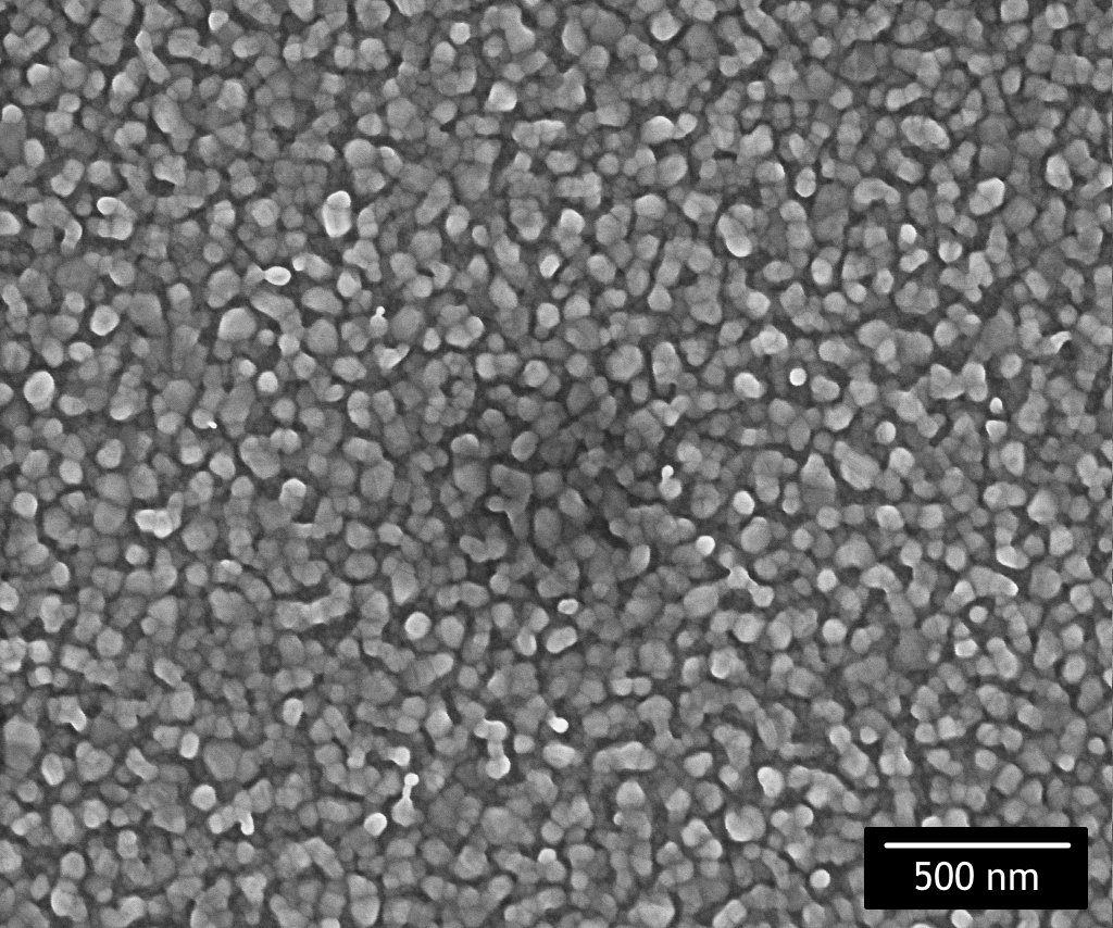
Sputter coating is a specialized sputtering system designed specifically for coating samples to improve imaging performance in scanning electron microscopy. A sputter coater typically produces a 20 [nm] thick conformal coating of gold.
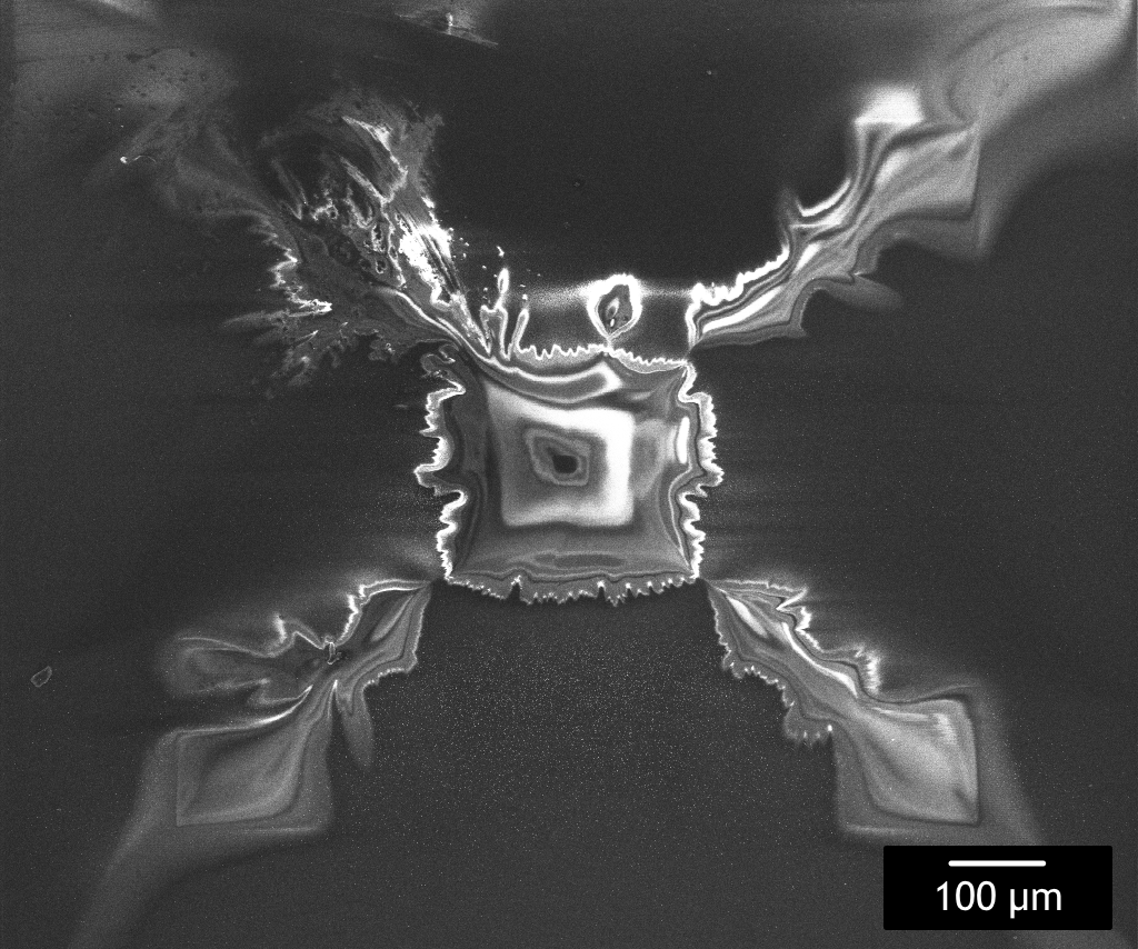
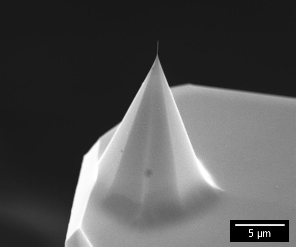
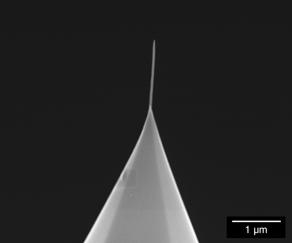
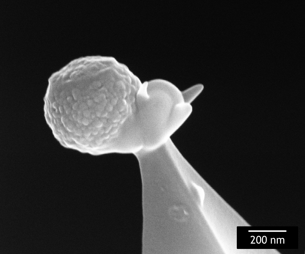
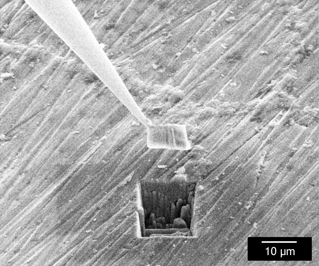
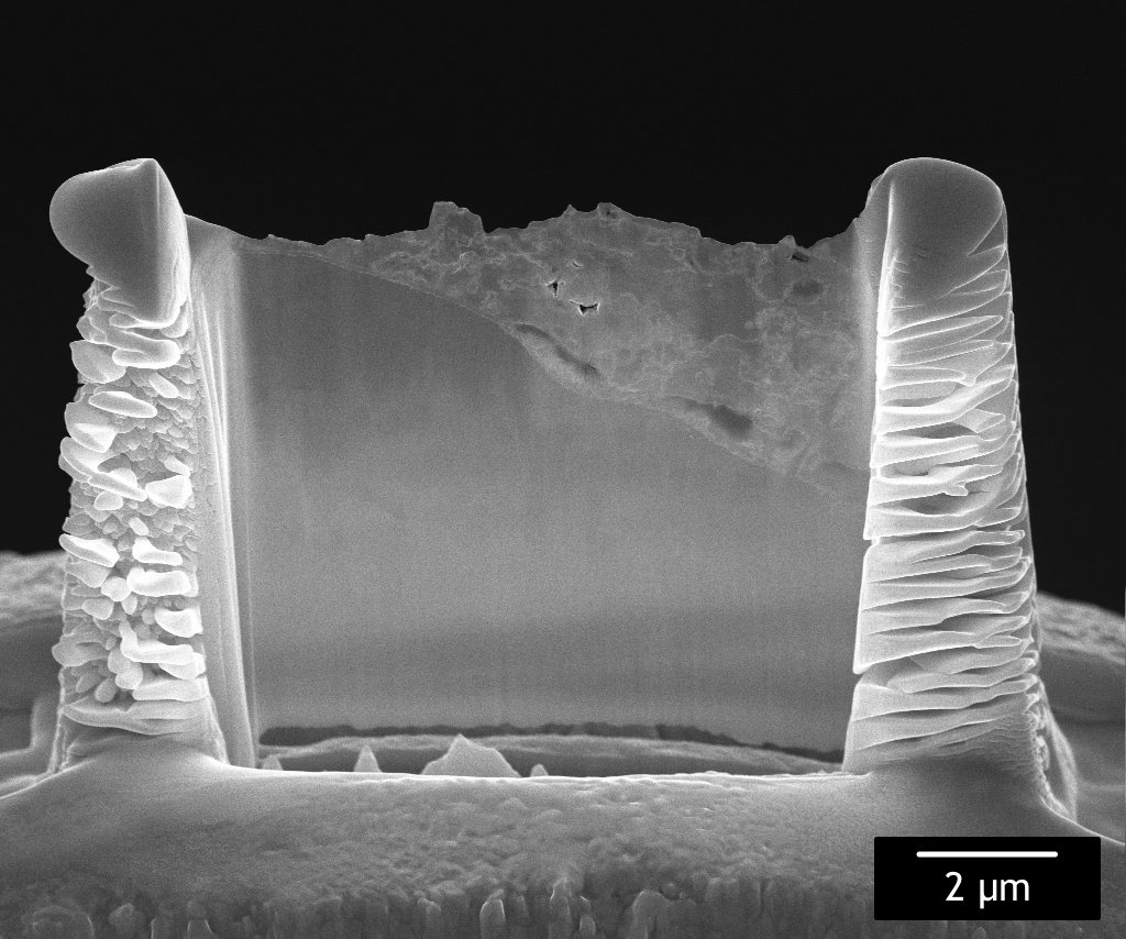
Focused ion beam decomposes a precursor material onto a substrate surface using a focused beam of ions. The precursor material is typically a gas that comprise of platinum that is chemically bound to an organic molecule. The focused ion beam locally heats up the surface which causes the precursor material in the vicinity to decompose into platinum and stick to the surface. This technique can deposit platinum patterns on a surface with less than 50 [nm] resolution.
Focused ion beam is typically used to deposit platinum to protect a sample from ion beam damage, grow platinum nano-needles, fix materials together, and connect conducting traces.