Microscopic gadgets are often fabricated on a tiny chip that needs to be connected to a large equipment for power and/or testing. A chip can be bonded and electrically connected to a printed circuit board to facilitate interfacing with other equipment. While it is possible to use UHNF to fabricate printed circuit boards, it is currently much faster, cheaper and more reliable to use a PCB prototyping service.
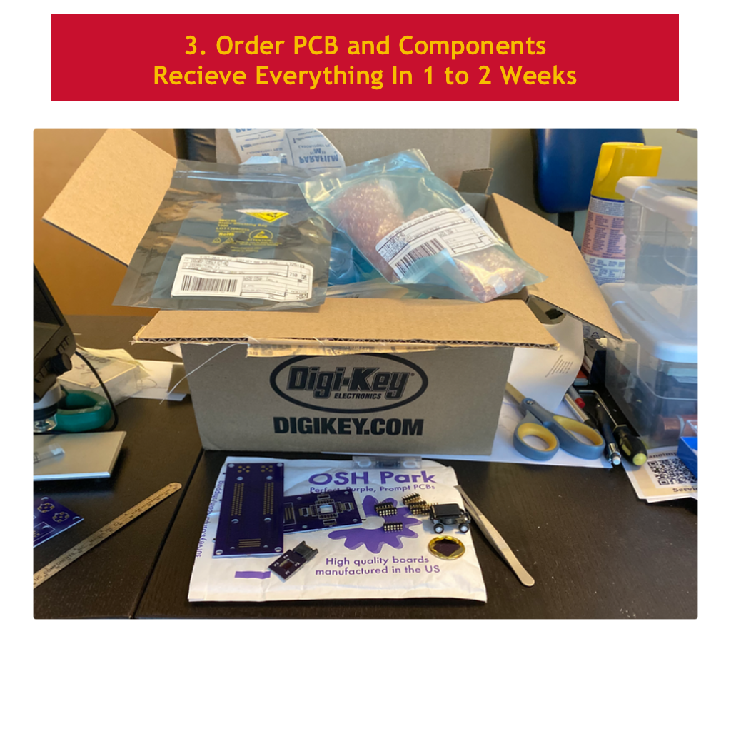
Printed circuit boards (PCB) are manufactured by companies to routine produce 150 [μm] minimum features. Individuals can get their design manufactured at a rate of $5 per square inch for a set of 3 pieces and delivered in less than 2 weeks.
How It Works
1. Design the PCB using DipTrace
DipTrace is a schematic and PCB design software. The freeware version provides the least restriction compared to competing software.
2. Upload it to OSHPark
OSHPark is a community service that provides printed circuit board manufacturing in prototyping volumes at an affordable price. They support 2-Layer, 4-Layer, Flex and more.
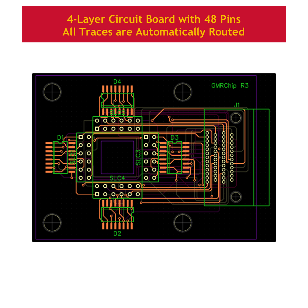
Examples
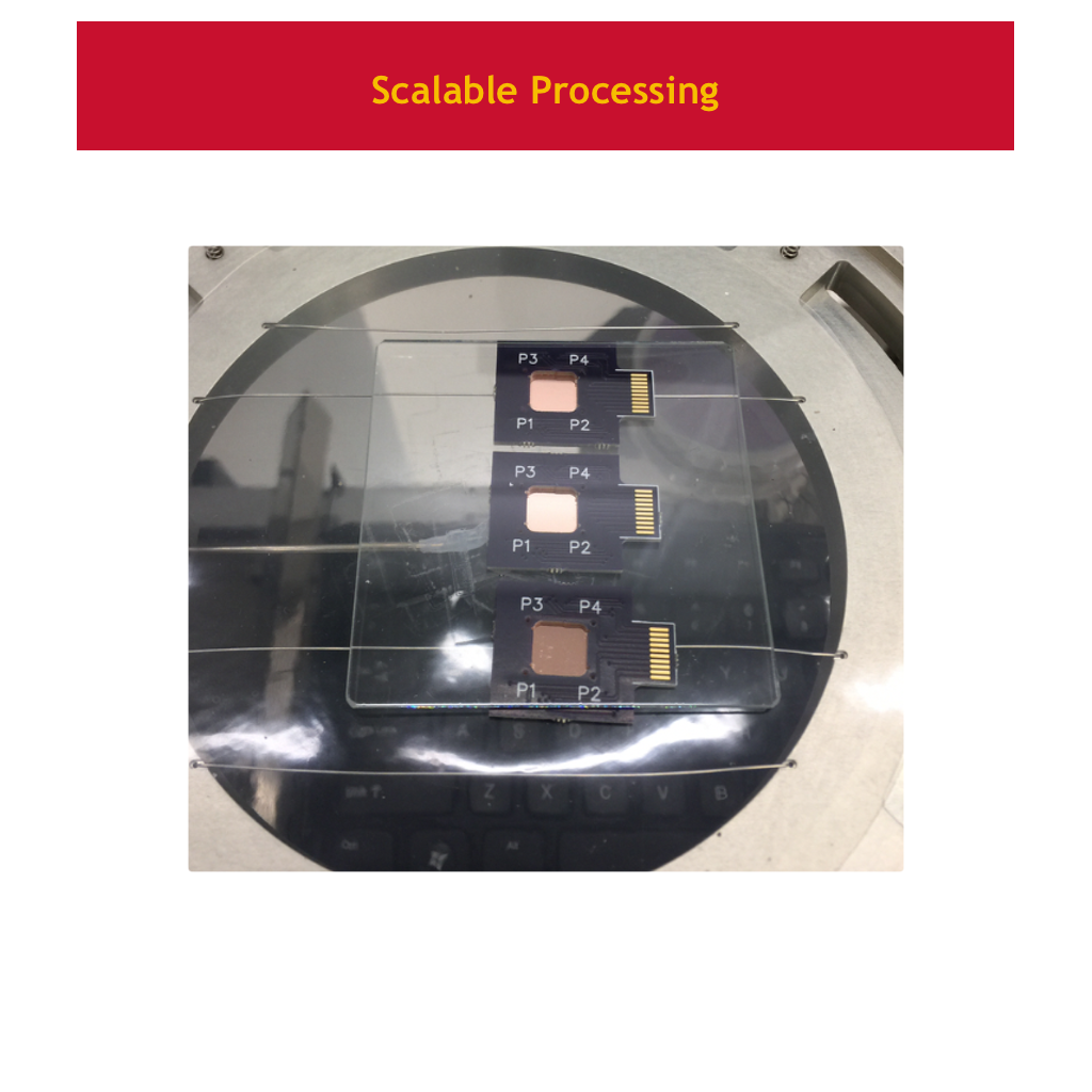
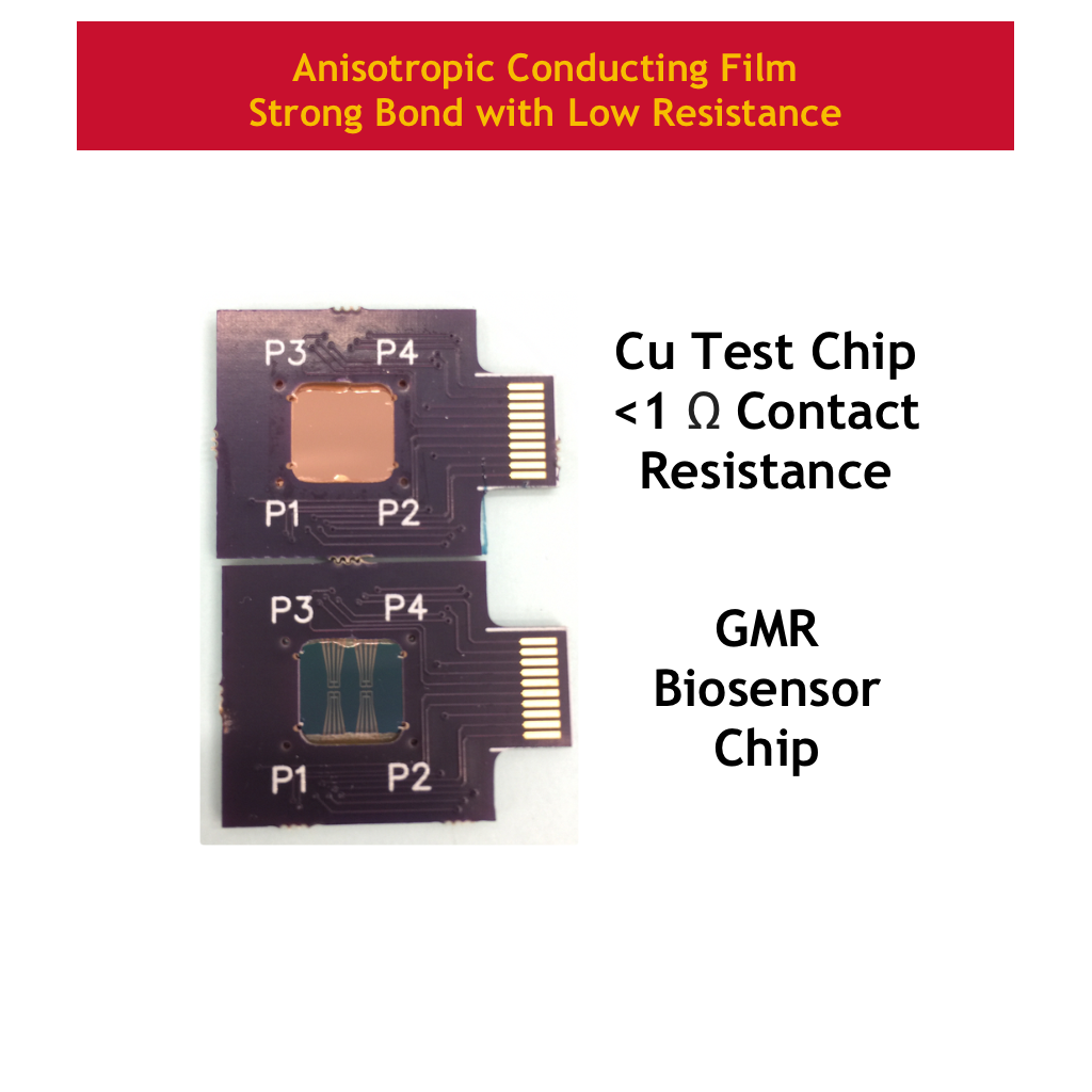
GMR Chip Packaging
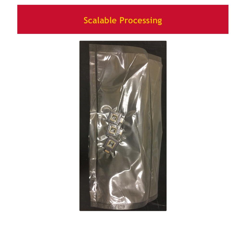
Dr. Litvinov, Professor of Electrical and Computer Engineering at the University of Houston, needed a scalable method to package their GMR biosensor chip for consumer use. One approach is to provide the chip with a USB-like interface so that after a test is performed, it can be inserted into a reader to acquire the results. The chip is connected to the PCB using an anisotropic conducting film (ACF).
The PCB chip contacts is cleaned with alcohol before applying the ACF. The ACF is then melted at 50 °C on a hotplate and pressed to improve adhesion and coverage. After cooling to room temperature, the chip is aligned to the PCB. Then the chip and PCB is placed in a vacuum sealed bag and baked in an oven at 100 °C for 5 minutes. This cures the ACF and produces a very strong bond and contact resistances below 1 Ω.
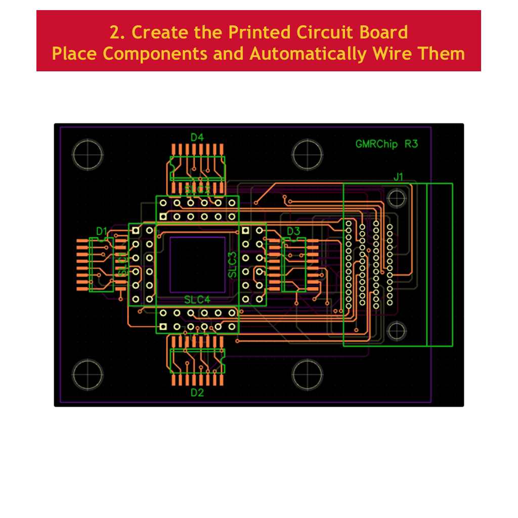
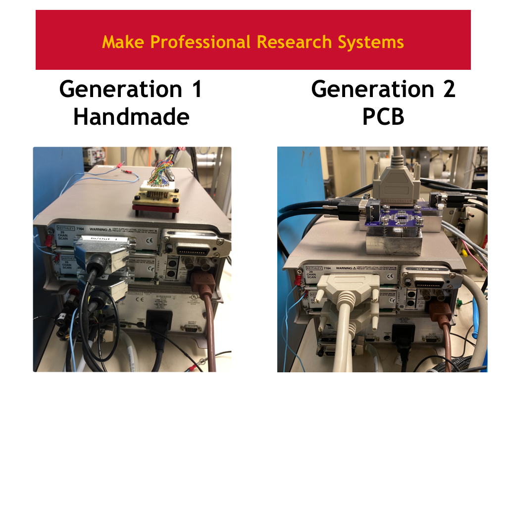
GMR Tester Chip Interface
Dr. Litvinov, Professor of Electrical and Computer Engineering at the University of Houston, needed a more robust method to test their GMR sensors. GMR sensors are very fragile and often gets damaged when electrical contacts are being applied. The first generation of the GMR test system was hand made, the wirings are complex and it is impossible to repair. We designed the second generation using commercial cables and printed circuit boards. Generation 2 looks professional, failed components can be replaced and it also provides electrostatic discharge protection.
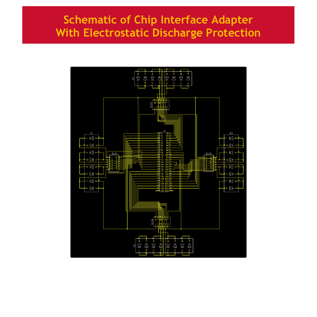
The chip interface board uses an array of 48 spring loaded contacts to provide temporary contacts to the GMR sensors. The spring loaded contacts are connected to shunting diodes to protect the sensors from electrostatic discharge damage. A low profile connector is used to connect the chip interface board to an adapter board. The adaptor board interfaces the low profile connector to a standard connector used by the scientific instrument.